CASE STUDY · AI SEMICONDUCTOR HARDWARE · SILICON WAFER LASER MICROMACHINING
Nine years of precision laser micromachining. From first holes in silicon to a $4M production ramp-up.
- Customer: A leading AI semiconductor company
- Application: Precision laser micromachining of silicon wafers for AI semiconductor hardware
- Duration: Nine years — prototype through to full production
Customer co-investment
In production ramp-up and systems
Product cost reduction
Through process optimisation
Production demand growth
Over the ramp period
Systems in service
By end of 2026, 8 more in build
THE BEGINNING
A few holes. A grand vision.
Nine years ago, Goodfellow Corp then Potomac Photonics began working with a leading AI semiconductor company on a technically demanding new application: precision laser micromachining of silicon wafers for a new generation of AI semiconductor hardware. What began as drilling a few holes in silicon substrates has since grown into a deep collaborative partnership now in full production.
In the early stages, our customer was developing and refining the product. Potomac worked alongside their engineering team on the laser micromachining requirements conducting process tests, producing silicon wafer samples, adjusting parameters, and iterating until the process was right. The collaboration was genuine from the start. Both teams communicated openly, not just presenting problems but bringing solutions. New silicon substrate designs and test requirements were turned around quickly.
The engineering questions evolved as the product evolved. Were the wafers flat enough? What dimensional tolerances could and needed to be held? What did the heat-affected zone do to the surrounding silicon material? How tight did the registration need to be across the wafer? How would the laser micromachining process scale to production volumes? With each challenge came collaboration and new solutions.
THE TURNING POINT
From beautiful parts to scalable production.
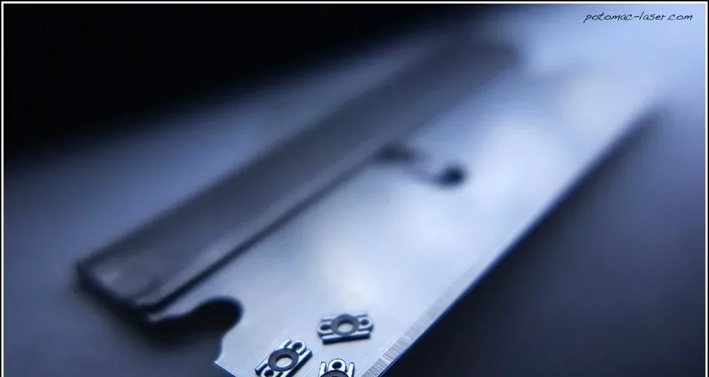
The early laser micromachining process was focused on quality producing the cleanest holes in silicon with minimal heat-affected zone. The results were excellent. But each silicon wafer was taking 6.0 to 7.5 hours to process. That was not scalable to production volumes.
Then, a little over four years ago, came the leap to ultrafast laser technology. Combining ultrashort pulse laser capability with years of accumulated process knowledge, the team developed ideal laser micromachining parameters for the silicon substrate application. In a co-funded effort, a custom, dedicated ultrafast laser system was designed and built specifically for this project.
The results were immediate. Those 6–7.5 hour silicon wafer processing times came down to 4 hours. Faster laser micromachining cycle times drove the part price down, bringing the project closer to production cost targets. Further process development over the following year shaved another hour or more from the cycle time. Product costs came down by 4×. As our customer’s AI hardware product gained traction in the market, production demand grew rapidly. A second custom laser micromachining system was added a little over a year ago to increase throughput and meet new volume targets.
Novel coating and cleaning methods were developed for the silicon wafers to ensure process consistency and substrate quality. A cleanroom was introduced to prevent contamination of the finished semiconductor components. Short production runs began alongside continued R&D to further refine the laser micromachining process.
“Eight years of emails, video conferences, late nights, and weekends. Whatever it took.”
Mike Davis, Vice President of Engineering, Goodfellow Corp.
WHERE WE ARE TODAY
A $4M co-investment and a technology ready to change its industry.
Then came the moment the whole partnership had been building toward. our customer was ready to move from small production runs to a full commercial launch of their AI semiconductor hardware. In a co-funded commitment of over $4M, the customer enabled Goodfellow to acquire all the equipment needed to build custom laser micromachining systems in-house to handle full production volumes while continuing to test and develop process improvements.
Ten custom laser systems will be in service before the end of 2026, with eight more currently in build. Production demand for the silicon wafer laser micromachining process is increasing by more than 6× over the ramp period. Supply chain logistics have been coordinated to ensure a secure, uninterrupted workflow throughout.
What began with a handful of precision-drilled holes in a silicon substrate is now a production programme at scale built on nine years of collaboration, laser micromachining expertise, and shared investment in getting it right.
The Goodfellow group advantage
Potomac Photonics joined the Goodfellow group in June 2024. The acquisition means a single partner now covers the entire workflow:
- Materials supply — 170,000+ specialist materials including substrates, coatings, and films for advanced semiconductor fabrication
- Precision laser micromachining — 40+ years of contract manufacturing expertise, from silicon wafer prototype through to production at scale
- Laboratory validation — Suisse Technology Partners AG, ISO 17025-accredited, FDA and Swissmedic acknowledged, provides independent analysis and process validation
Source the material. Machine the part. Validate the output. One group, one workflow.