What is Laser Patterning?
Laser patterning is a high-precision, maskless process that uses focused laser energy to selectively remove or modify surface materials with micron-level accuracy. This direct-write approach eliminates the need for stencils or photomasks, making it ideal for delicate or complex substrates.
By carefully controlling laser wavelength, pulse duration, and energy, Potomac can produce intricate patterns, define thin-film circuits, or selectively remove coatings while preserving the integrity of the underlying material. The process is non-contact, repeatable, and capable of features down to a few microns.
Applications of Laser Patterning
Precision Circuitry and Thin Films
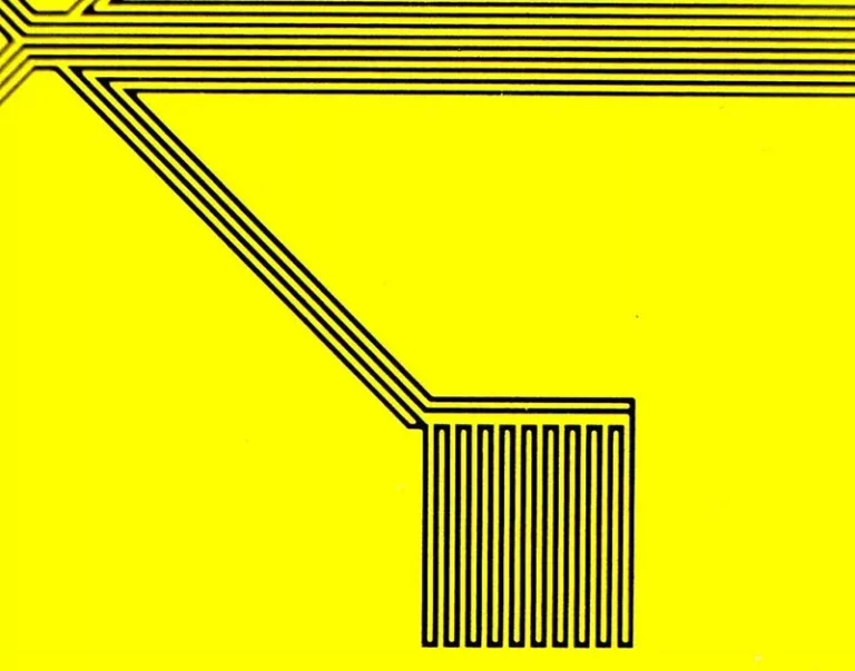
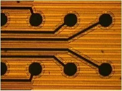
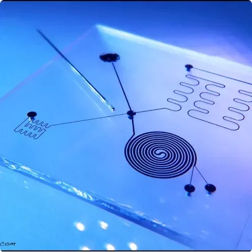
Laser patterning can define conductive or isolating paths on thin-film materials, making it suitable for microelectronics, sensors, and flexible circuits. By adjusting the laser parameters, we can pattern both conducting and insulating areas with micron-scale accuracy.
Surface Functionalization
Patterned surface structures can alter physical or chemical properties, such as hydrophobicity, adhesion or optical response, without introducing additional materials or coatings. This capability supports advanced components in optics, biomedical devices, and functional surfaces.
Coating Removal and Material Isolation
Many precision devices require selective removal of surface coatings while leaving the substrate intact. Potomac’s laser patterning processes can rapidly remove large areas or produce fine, controlled patterns in coatings such as aluminum on polyimide with micron-level precision.
Custom and Prototype Patterns
Because the process is driven directly from CAD files, design changes can be implemented quickly without the cost or lead time of photomasks or tooling. This makes laser patterning ideal for prototyping, iterative design work, and short production runs.
Industries we serve
✦ Electronics & Flexible Circuits
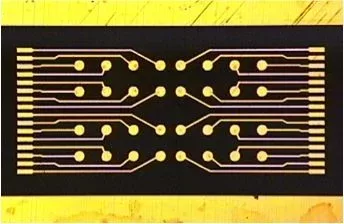
Laser patterning is widely used to define conductive traces, remove metal layers, and create fine-pitch circuit features on flexible substrates like Kapton (polyimide) and Mylar. Common applications include patterning aluminum or copper on polymer films for flex circuits, antennas, and transparent conductive electrodes (ITO or AgNW on PET). Because the process is maskless and driven directly from CAD files, design iterations are fast and cost-effective — ideal for prototyping new interconnect architectures or moving quickly to small production runs.
Typical use cases: Flex circuit patterning, ITO electrode removal, wire stripping, via preparation, thin-film resistor trimming.
✦ Microfluidics & Lab-on-a-Chip
Laser patterning complements microfluidic device fabrication by creating hydrophilic/hydrophobic contrast zones, defining electrodes for electrokinetic flow control, or removing surface coatings to expose specific materials for bonding or functionalization. When combined with Potomac’s laser micromachining and hot embossing capabilities, laser patterning enables fully integrated, end-to-end microfluidic chip production.
Typical use cases: Electrode patterning for electrophoresis chips, surface treatment zoning on PDMS or PMMA chips, patterned adhesion layers for multi-layer laminate assembly.
✦ Photovoltaics & Energy Devices
In solar cell and thin-film battery manufacturing, laser patterning is used to scribe and isolate layers — removing transparent conductive oxides (TCO), metal back contacts, or active semiconductor films with precise edge definition. The process enables cell-to-cell isolation scribing and contact pad definition without contamination from wet chemistry.
Typical use cases: TCO scribing on thin-film solar panels, isolation scribing on perovskite or CIGS cells, current collector patterning on flexible batteries and supercapacitors.
✦ Medical Devices & Diagnostics
In the medical device industry, laser patterning delivers the micron-level precision required for electrodes, biosensor arrays, and implantable components. Selective removal of metallic or polymer coatings on catheters, guidewires, and neural probes enables functional zoning — exposing only the desired active areas while protecting surrounding material. The non-contact, dry process eliminates chemical contamination risks important for biocompatible and ISO 13485-compliant manufacturing.
Typical use cases: Electrode definition on implantable leads, patterning of sensor arrays on catheters, ablation of insulating coatings on medical-grade wires.
Why Choose Potomac for Laser Patterning?
Potomac Photonics combines decades of process development with advanced laser systems capable of delivering high-resolution patterning across a wide range of materials. Our engineers partner with customers early in the design and manufacturing process to recommend the best laser parameters and strategies tailored to your material, geometry, and production needs.
With direct access to over 170,000 advanced materials, Potomac can support virtually any substrate, from metals and polymers to ceramics and specialty composites. This breadth of material availability allows us to tackle complex and diverse patterning projects without the delays associated with sourcing rare or specialized materials.
In addition, we provide rapid turnaround for prototyping and production runs, helping customers accelerate development cycles and meet tight project timelines. From isolating thin films and defining micro-features to functional surface modifications and coating removal, laser patterning at Potomac delivers precision, flexibility, and repeatability that support both prototype and production requirements.
Need Additional Microfabrication?
Potomac offers generous incentives to our customers that combine laser patterning with our exhaustive list of other microfabrication processes.
Also From the Goodfellow Group
Laser patterning of thin films and functional coatings requires substrates with consistent surface quality and layer uniformity. Goodfellow supplies Kapton, metallized Kapton, coated glass, copper foil, and a wide range of patternable films and substrates.
Source Kapton, metallized films, and coated substrates from Goodfellow.
Coating removal uniformity, residual layer thickness, and substrate surface chemistry after laser ablation can be confirmed through Goodfellow’s ISO 17025-accredited materials testing division using XPS or EDX analysis.
Verify patterning quality and coating integrity with accredited surface analysis.