
Material Spotlight: Silicon
Potomac has spent many years developing and optimizing laser cutting and drilling of silicon wafers for a broad range of applications. In this article we examine this unique material. Swedish chemist Baron…
Potomac has spent many years developing and optimizing laser cutting and drilling of silicon wafers for a broad range of applications. In this article we examine this unique material.
Swedish chemist Baron John Jacob Berzelius first isolated Silicon in 1824. The shimmering blue and gray element is as fascinating as it is plentiful: it is the second most common element on earth, and the eighth most common in the universe. The word “Silicon” is from the Latin word “Silex for Flint.” Sharp flint tools derived from quartz, which contains silicon were made by Stone Age humans. Scroll ahead 500,000 years, and you will find the demand for silicon for consumer electronics has skyrocketed. Like carbon one of its fellow family members in Group 14 of the Periodic Table, silicon is something of a paradox. It appears in many different forms in nature often alloyed with other materials, such as oxygen. It is in this state that we find sand, silicon dioxide. Another substance that contains silicon is, of course glass. And while carbon is the building block of all life on earth, silicon is a building block of one form of life. Diatoms are photo synthesizing algae whose cell walls are made of silicon.
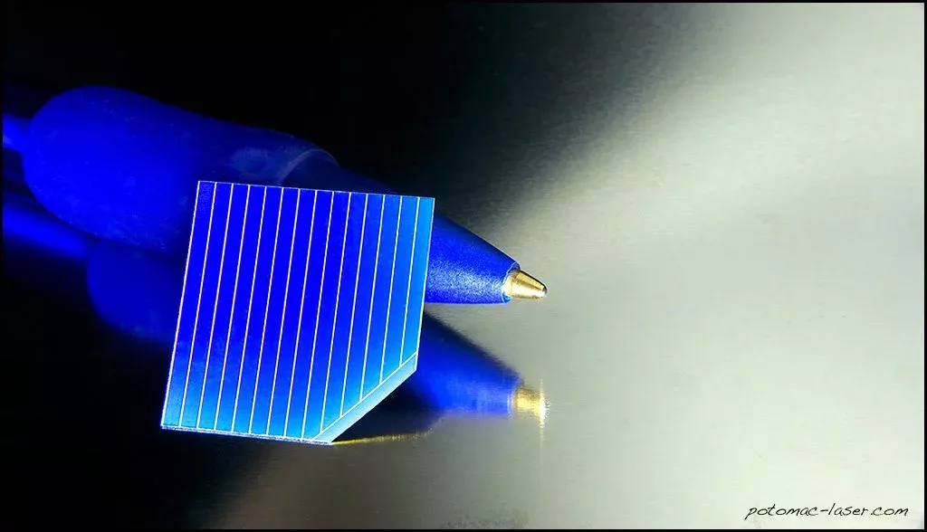
Whether silicon will one day be identified as the building block of alien life, as in the imaginations of science fiction writers from Issac Asimov to Star Trek’s Gene Roddenberry is a question yet to be answered. The truth remains that here on earth, the forms of silicon that power our consumer electronics, solar cells, and even our artificial intelligence are the single crystal form – monocrystalline silicon, polycrystalline form, and amorphous silicon. The first is chemically “grown” through an elaborate process, the Czoralski method. Polish chemist Jan Czoralski developed this after mistakenly dipping a fountain pen into a crucible of liquid tin instead of his inkwell and finding that the solid piece of tin that instantly formed was a solid crystal. Polycrystalline silicon is created through the Siemens method, which distills and decomposes silicon compounds into silicon at high temperatures. It can also be chemically engineered in a fluidized bed reactor. Crystallized silicon is made into silicon wafers, with the addition of the elements phosphorous and boron in a process called “doping.” These wafers are semiconductors and the electrical brains for many of our favorite things. Sales by the semiconductor manufacturing industry (led by Intel), reached $409 billion dollars in 2017 and are projected to grow.
From personal computers, to laptops and tablets, phones to smart televisions, digital cameras and my personal favorite the iphone compatible, blue tooth enabled shower speaker, silicon is king.
Artificial intelligence is also advancing steadily, and it holds great promise in the field of health care. Already, there are artificial intelligence programs that collect, store and analyze medical data and which utilize neural networks to detect information that may be invisible to human diagnosticians.
Sensor technology has also made a leap forward from smart home appliances such as washing machines, dishwashers, water heaters that can communicate with the customers, the power grid and with one another to conserve resources and save money.
Exciting to Potomac is also the further development of photovoltaic technology. Smart windows can block and attract solar heat with photo solar cells. And the near future will bring solar powered cars.
According to Dr. Ethan Miller, my friend and Professor in the Computer Engineering department of the University of California, Santa Cruz, light- photovoltaic energy, created with silicon laser semiconductors may soon replace electricity to power our silicon semiconductors. At 186,000 miles per second, it’s faster than electromagnetic waves. And because it runs on less power, it is surprisingly energy efficient.
As to my question about whether an intelligent silicon based life form is possible, Dr. Miller answered that when scientists are able build a computer that is as smart as the human brain, a silicon based life form will be created.
Silicon will live on!
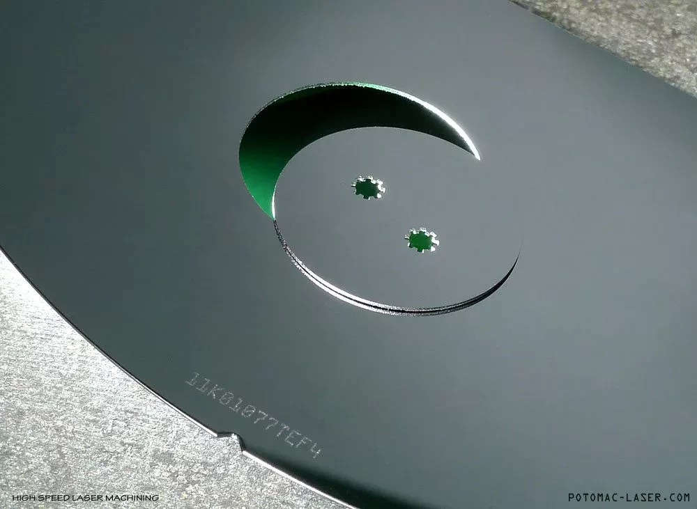
With capabilities ranging from drilling very small holes to laser cutting complex shapes, Potomac is the leader in laser fabrication of silicon. Please Email or call us today to discuss your next prototyping or production silicon wafer application.
Potomac, NASA and Small Parts….
Potomac Photonics has been collaborating with our friends at NASA for years. In fact, it was a set of Small Business Innovation…
Read article → 3D Printing
 Revolutionizing Leak Testing / Container Closure Integrity (CCIT) with Potomac Photonics’ Rapid Turnaround Hole Drilling Capabilites
Container Closure Integrity Testing (CCIT) is crucial for ensuring the sterility and safety of packaging in pharmaceutical and other critical industries. Potomac…
Read article →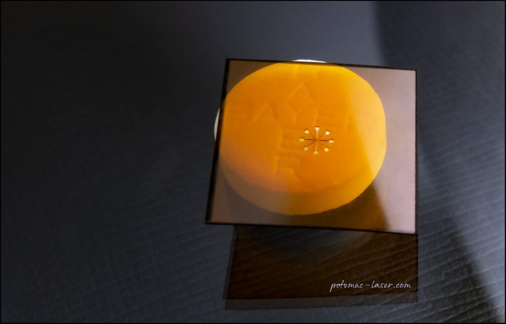 3D Printing
 DuPont Kapton Polyimide: Versatile Applications and Potomac Photonics’ Expertise in Laser Micro Machining
Introduction DuPont’s Kapton polyimide is a high-performance polymer known for its exceptional electrical insulation, mechanical strength, and resistance to extreme temperatures and…
Read article →Ready to discuss your next micromachining project?
Reach the Potomac Photonics engineering team to talk through process and qualification requirements. Upload STEP, STL, or PDF — our engineers review it for manufacturability.
No commitment · Our engineers respond within 24 hours