
Micro Electronics Manufacturing
Potomac’s broad-range of micro manufacturing technology includes a novel technique to embed conductive materials in a wide variety of substrates. Using laser-based processes, Potomac can produce fine-feature groove and channel patterns in…
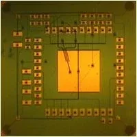
Potomac’s broad-range of micro manufacturing technology includes a novel technique to embed conductive materials in a wide variety of substrates.
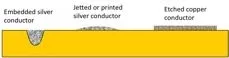
Using laser-based processes, Potomac can produce fine-feature groove and channel patterns in many electronics and display substrate materials. We can then fill these etched patterns with a nanoparticle silver paste which is cured at low temperatures to produce fine-feature conductor patterns embedded into the substrate.
The cured nanoparticle materials exhibit high electrical conductivity, and minimum feature sizes can be 10 microns or less. Aspect ratios (height/width) can be larger than 1. Conductors with these characteristics are difficult to fabricate with conventional jet-printing or etching processes.
Conductor patterns can be fabricated on both top and bottom of the substrate with silver-filled vias providing connections between them. The combination of fine feature sizes and a via interconnect capability gives embedded nanosilver conductor technology a significant advantage in many applications
 Industry
 Machining Kapton for Aerospace: Precision That Survives the Environment
Kapton polyimide is one of the most specified materials in aerospace — and one of the most demanding to machine correctly. Why…
Read article → Company
 Why Every Part Matters: Our Commitment to Customers, Innovation, and Impact
A Letter From Our Team: Why We Feel Every Project Matters At Potomac Photonics, we do not just manufacture parts. We help…
Read article →
Articles Material Spotlight: DuPont™ Kapton® – A Powerhouse for Micro Manufacturing
Over the next few months, we are going to profile different materials that are optimized for micro manufacturing. This includes both rapid…
Read article →Ready to discuss your next micromachining project?
Reach the Potomac Photonics engineering team to talk through process and qualification requirements. Upload STEP, STL, or PDF — our engineers review it for manufacturability.
No commitment · Our engineers respond within 24 hours