

 Lanham, MD, July 31, 2012: Leading micromachining provider, Potomac Photonics, has added a new laser system capable of high speed machining of polycrystalline silicon material. The process is optimized for small hole drilling and high precision cutting applications.
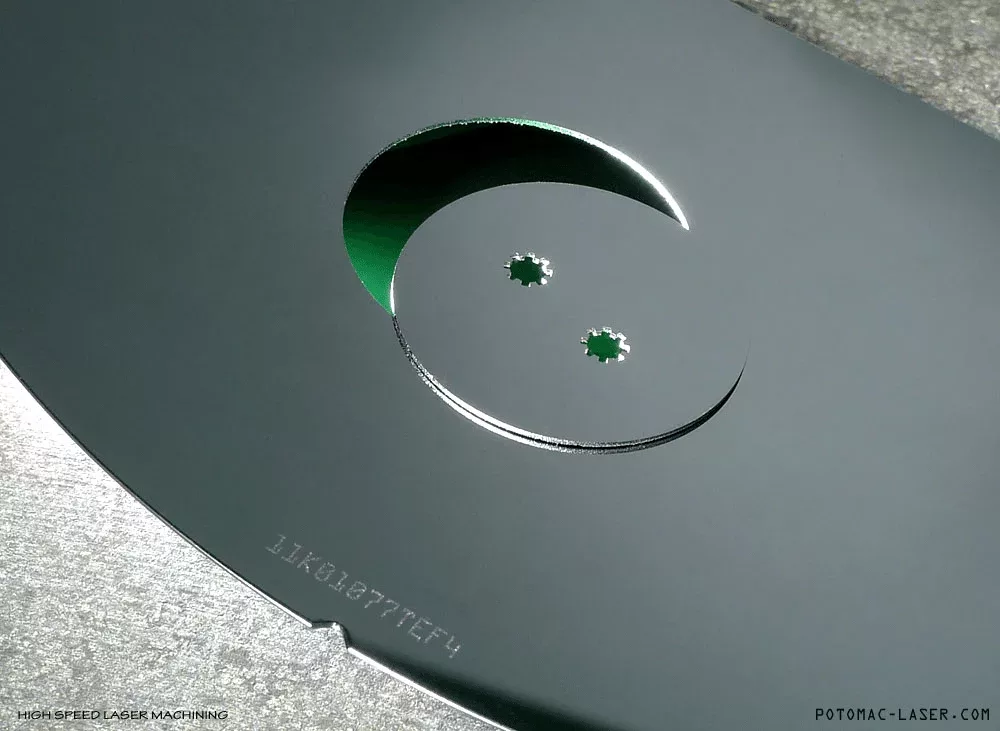
Silicon wafer cutting capabilities include:
- 150 microns achieved in materials as thick as 1mm
- Extremely smooth edges and minimal micro fractures
For customers requiring smaller features, Potomac’s machines can drill as small as 25 microns.
“We are very pleased to add this high-speed silicon wafer cutting process to our expanding list of micromachining capabilities,” says Greg Behrmann, Chief Technology Officer, Potomac Photonics.
Industries that can benefit from this new laser technology include medical devices, biotech, electronics, alternative energy, automotive and consumer goods. Potomac Photonics is ISO 9001:2008 and ISO 13485:2003 certified.
Potomac Photonics is a leader in microhole drilling. For more information on capabilities and processes, visit https://www.potomac-laser.com.
ABOUT POTOMAC PHOTONICS
Potomac Photonics is a leader in microfabrication helping clients with prototyping to production to develop miniature products and bring them to market. Potomac is an authorized distributor for high-tech manufacturing technologies including 3D printers and laser systems. With cutting-edge manufacturing technology, Potomac is recognized by both commercial and government agencies for innovation in medical devices, electronics, aerospace, and automotive manufacturing. Potomac’s high-tech facility, located in Lanham, MD, is ISO 9001:2008 and ISO 13485:2003 certified. Visit www.potomac-laser.com