
Potomac Photonics R&D Working on Nanoimprint Lithography and Applications for Microfluidics
Nanoimprint lithography is a method by which nanoscale features are fabricated at potentially low cost and with high throughput patterning usually in thermoplastics. Over the past 20 – 30 years this technology…
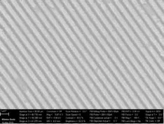

Nanoimprint lithography is a method by which nanoscale features are fabricated at potentially low cost and with high throughput patterning usually in thermoplastics. Over the past 20 – 30 years this technology has rapidly developed into a legitimate lithographic technology that has found application within several industries, mainly Photonics, Semiconductors, microfluidics, and biomimetic substrate structures 1. Nanoimprinting requires a nanoscale mold that defines the features and structures that are transferred to a final device or material. These nanoimprinting molds can be produced using several different methods depending on their specific application, most commonly used methods are Electron beam lithography (EBL), Laser writing, Deep UV lithography (DUV) and Reactive etching methods (like Reactive ion etching (RIE), Inductively coupled plasma (ICP) etching among other methods 2. These nanoimprint molds are then used to produce relief structure in various pattern transferrable or embossable materials, thus generating the final devices.
Together with the Research and Development labs at Potomac Photonics Inc., researchers at NCAT, look to commercialize this technology for Stem cell research. Nanoimprinting molds were purchased from LightSmyth Technologies (http://www.lightsmyth.com/product/nanopatterned-silicon-stamps/) and used for embossing patterns into thermoplastics using methods developed at Potomac Photonics Inc (Figure A and B). The scope of work in this project includes the proof of concept, selection and development of manufacturing techniques and methods required for the hot embossing and rapid prototyping of nanoimprints in polymers. Potomac Photonics Inc. is working closely with Prof. Salil Desai to specify and optimize conditions for the nanoimprint technology for use in Stem Cell differentiation studies and scale-up of this technology into production and manufacturing. An optimal method based on performance and manufacturability will be identified, where, facilities, services, engineering and materials are provided for rapid prototyping, process development and scale-up of these devices by iterative development between Prof. Salil Desai (NC A &T SU) and Potomac. Potomac Photonics Inc. specializes in hot embossing and device fabrication, with client services for feature sizes ranging from 100 nm – 1 mm for nanoimprinting. Current technologies have seen an increase in nanopatterning for industries such as Pharmaceuticals, Photonics, electronics, etc. Now, together with Prof. Salil Desai we hope to make this available to the Biopharmaceutical and Stem cell technologies markets.
Reference:
- Kumar CSSR, Hormes J, Leuschner C. Nanofabrication Towards Biomedical Applications. Vol 34.; 2005. doi:10.1002/3527603476
- Barcelo S, Li Z. Nanoimprint lithography for nanodevice fabrication. Nano Convergence. 2016;3(1). doi:10.1186/s40580-016-0081-y
Potomac, NASA and Small Parts….
Potomac Photonics has been collaborating with our friends at NASA for years. In fact, it was a set of Small Business Innovation…
Read article →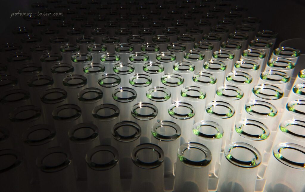 3D Printing
 Revolutionizing Leak Testing / Container Closure Integrity (CCIT) with Potomac Photonics’ Rapid Turnaround Hole Drilling Capabilites
Container Closure Integrity Testing (CCIT) is crucial for ensuring the sterility and safety of packaging in pharmaceutical and other critical industries. Potomac…
Read article →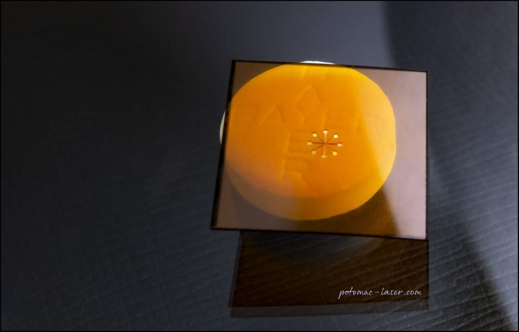 3D Printing
 DuPont Kapton Polyimide: Versatile Applications and Potomac Photonics’ Expertise in Laser Micro Machining
Introduction DuPont’s Kapton polyimide is a high-performance polymer known for its exceptional electrical insulation, mechanical strength, and resistance to extreme temperatures and…
Read article →Ready to discuss your next micromachining project?
Reach the Potomac Photonics engineering team to talk through process and qualification requirements. Upload STEP, STL, or PDF — our engineers review it for manufacturability.
No commitment · Our engineers respond within 24 hours