
Laser Drilling of Port Holes for Microfluidic Devices
Microfluidic devices are a type of miniaturized lab-on-a-chip technology that have been gaining popularity in recent years. These tiny devices are used to manipulate and analyze very small quantities of fluids, and…

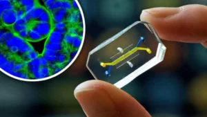
 Microfluidic devices are a type of miniaturized lab-on-a-chip technology that have been gaining popularity in recent years. These tiny devices are used to manipulate and analyze very small quantities of fluids, and they have a wide range of applications in fields such as medicine, chemistry, and biology. One of the key components of microfluidic devices is the port hole, which allows for the introduction of fluids and the collection of data.
Traditionally, port holes for microfluidic devices have been created using techniques such as micromilling or chemical etching. While these methods can produce high-quality port holes, they can be time-consuming and expensive, and they may not be suitable for certain materials such as thermoplastics or glass.
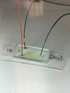
Fortunately, there is a new technology that is revolutionizing the way port holes are created for microfluidic devices: laser drilling. Laser drilling involves using a highly focused laser beam to vaporize material and create a precise hole. This technique is incredibly precise and can produce holes with diameters as small as a few microns.
 One of the main benefits of laser drilling is that it can be used to create port holes in a wide range of materials, including thermoplastics and glass. This is because the laser can be tuned to the specific properties of the material being drilled, ensuring that the hole is created cleanly and accurately without damaging the surrounding material.
Another advantage of laser drilling is that it is fast and cost-effective. Because the process is automated, it can be completed quickly and without the need for expensive tooling or equipment. This means that microfluidic devices can be produced more quickly and at a lower cost, making them more accessible to researchers and scientists.
Perhaps most importantly, laser drilling allows for greater design flexibility when it comes to port holes for microfluidic devices. Because the process is so precise, it is possible to create complex port hole patterns that would be difficult or impossible to achieve using traditional methods. This opens up new possibilities for the design of microfluidic devices and could lead to exciting new discoveries in fields such as medicine and biology.
 In conclusion, laser drilling is an exciting new technology that is transforming the way port holes are created for microfluidic devices. Its precision, versatility, and cost-effectiveness make it an ideal choice for researchers and scientists looking to create high-quality microfluidic devices quickly and efficiently. With laser drilling, the possibilities for innovation in this field are virtually limitless
Potomac Photonics is a leader in micro manufacturing with a broad range of technologies such as lasers, micro-CNC, micro 3D printing and a variety of bonding technologies. From prototyping to full scale production we look forward to learning more about your application. Please call or Email us today.
Potomac, NASA and Small Parts….
Potomac Photonics has been collaborating with our friends at NASA for years. In fact, it was a set of Small Business Innovation…
Read article → 3D Printing
 Revolutionizing Leak Testing / Container Closure Integrity (CCIT) with Potomac Photonics’ Rapid Turnaround Hole Drilling Capabilites
Container Closure Integrity Testing (CCIT) is crucial for ensuring the sterility and safety of packaging in pharmaceutical and other critical industries. Potomac…
Read article → 3D Printing
 DuPont Kapton Polyimide: Versatile Applications and Potomac Photonics’ Expertise in Laser Micro Machining
Introduction DuPont’s Kapton polyimide is a high-performance polymer known for its exceptional electrical insulation, mechanical strength, and resistance to extreme temperatures and…
Read article →Ready to discuss your next micromachining project?
Reach the Potomac Photonics engineering team to talk through process and qualification requirements. Upload STEP, STL, or PDF — our engineers review it for manufacturability.
No commitment · Our engineers respond within 24 hours