
From NASA Perseverance Laser Marking on Mars
Product marking and coding is one of the most successful applications of laser technology. Light engraves a wide variety of substrates quickly and economically and some wavelengths, like those in the ultraviolet,…

Product marking and coding is one of the most successful applications of laser technology. Light engraves a wide variety of substrates quickly and economically and some wavelengths, like those in the ultraviolet, allow for very small micro-marks. Etching a mark right into the surface of a product is a strong deterrent to counterfeiting since it cannot easily be removed as with ink marks. For the diamond industry, lasers are also used for identification to ensure stone authenticity, and many industrial applications exist creating fiduciary marks for assembly in products such as flat panel displays.
Product marking and coding is one of the most successful applications of laser technology. Light engraves a wide variety of substrates quickly and economically and some wavelengths, like those in the ultraviolet, allow for very small micro-marks. Etching a mark right into the surface of a product is a strong deterrent to counterfeiting since it cannot easily be removed as with ink marks. For the diamond industry, lasers are also used for identification to ensure stone authenticity, and many industrial applications exist creating fiduciary marks for assembly in products such as flat panel displays.
Now, laser marking is going to Mars!
Over the years there have been some space geek jokes about leaving graffiti on the moon or other planets, but now there is a real reason to mark and code rocks from Mars.
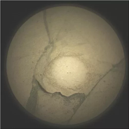
A particular team led by MIT in Cambridge, MA is studying Mars rocks returned to Earth after being collected by space traveling robot Perseverance. The scientists are especially interested in paleomagnetism, the study of the magnetism induced by the magnetic field at the time of the rock’s formation. For this research it is critical to know the orientation of the core sample when it was removed from a Mars rock. MIT Professor Ben Weiss had an idea for identifying each sample and contacted NASA to see if the laser onboard Perseverance could be used for marking the rock cores.
Tests by Los Alamos National Lab proved the concept was viable and now the NASA SuperCAM team is ready to deploy the laser marking robot into the wilds of the Red Planet.
Laser Marking Here on Earth
Back on Earth, Potomac has a wide range of technologies that can add clean, crisp codes and marks onto products in a wide range of materials. Possible substrates include metals such as stainless steel, gold, and silver, as well as organic polymers, plastics, ceramics, and diamonds or other gemstones.
Our unique capability to laser engrave thin glass substrates for applications like microfluidic devices with no cracking or thermal damage is especially noteworthy. Not only are our processes fast and efficient with automated quality control, we reduce the waste found in the trial and error of inexperienced in-house operations.
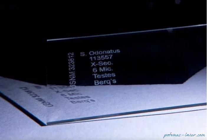
Potomac’s expertise working on tiny spatial scales as small as one micron, also gives us the ability to micro-mark medical devices or micro-electronics. This is an elegant solution for eliminating labels that are prone to being detached from the product.
While most of our work is here on our home planet, we’ve let NASA know we’re standing by if needed!
Learn more about our precision advanced manufacturing capabilities at potomac-laser.com. We innovate processes that rocket new products from Prototype to Production at warp speed.
 Industry
 Machining Kapton for Aerospace: Precision That Survives the Environment
Kapton polyimide is one of the most specified materials in aerospace — and one of the most demanding to machine correctly. Why…
Read article →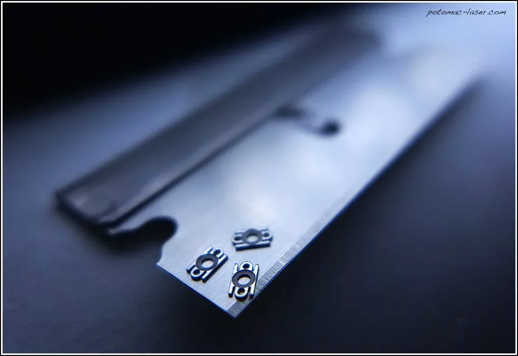
Patience and partnership on the path to production
Nine years of precision laser micromachining. From first holes in silicon to a $4M production ramp-up.
Read article →
All In
We are all in together so we can be all in for our customers. Last week a group of us from the…
Read article →Ready to discuss your next micromachining project?
Reach the Potomac Photonics engineering team to talk through process and qualification requirements. Upload STEP, STL, or PDF — our engineers review it for manufacturability.
No commitment · Our engineers respond within 24 hours