
激光直写技术及其低加工温度低成本应用
-Article By David Lui Laser direct-write is a new processing technology that allows the rapid fabrication of micro devices and circuits. These micro devices and circuits find applications in a variety of…
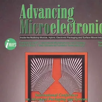
-David Lui 撰文
激光直写是一种新型加工技术,可以快速制造微型器件和电路。这些微型器件和电路可应用于微电子、光子学、MEMS 和 MOEMS 等各种领域。该技术采用低温加工(200-350°C),无需使用掩模、丝网、模具或印章。它还避免使用光刻胶和复杂的化学品,从而避免相关成本和潜在的环境影响。激光直写技术能够产生尺寸小至几微米的特征。
如今,微电子行业有两种主流加工技术:厚膜和薄膜。厚膜技术利用成像屏幕将材料打印在基板上,然后
通过在高温下烧制,通常在 800-1200°C 之间。使用连续的丝网印刷和烧制工艺步骤来构建电路。厚膜技术已用于通过低温(-850°C)共烧陶瓷(LTC C)工艺制造多芯片模块(MCM)和 3-D 电路。厚膜技术无法轻松产生宽度小于 -100 毫米(0.004 英寸)的线和空间。

 文章
文章 材料聚焦:杜邦™ Kapton® - 微制造的动力源
Over the next few months, we are going to profile different materials that are optimized for micro manufacturing. This includes both rapid…
Read article → 3D 打印
3D 打印 波托马克、美国国家航空航天局和小零件……
Potomac Photonics has been collaborating with our friends at NASA for years. In fact, it was a set of Small Business Innovation…
Read article → 文章
文章 开拓新领域:反思 2024 年,拥抱 2025 年创新
Reflecting on 2024: One Micron at a Time As the new year begins, we are proud to reflect on all we accomplished…
Read article →Ready to discuss your next micromachining project?
Reach the Potomac Photonics engineering team to talk through process and qualification requirements. Upload STEP, STL, or PDF — our engineers review it for manufacturability.
No commitment · Our engineers respond within 24 hours