Microfluidic Fabrication

Rapid Fabrication of Microfluidic Devices from Prototyping to Full Scale Production
Potomac’s broad range of microfabrication tools and technologies has finally made the promise of microfluidic devices come true. Utilizing tools such as lasers, micro-CNC, hot embossing and micro-3D printing, Potomac has broken the barriers that prevented microfluidics from becoming mainstream. Our focus has been to create technologies that speed up the development process, lower the cost of prototypes, customizaiton and a strategy for ramp-up focused on meeting deadline and target production pricing.
Potomac’s turnkey microfluidic fabrication solutions include fabrication of the chips, multiple layer alignment, bonding and testing. During the initial stages of the project, Potomac will work closely to understand the customers requirements and come up with a plan that meets their short and long term goals. Topics often include material selection, design from manufacturability, price targets, quality/testing, timelines and other critical milestones.
Potomac Photonics will develop a robust, reliable and repeatable micromanufacturing process that achieves design and performance specifications and considers the scalability and economics for our customers microfluidic products and technologies. An iterative approach of design, fabrication and testing will enable flexible adaptation of the manufacturing technology to design modifications throughout the project.

Phase 1: Process Development
During process development the emphasis is to rapidly and flexibly fabricate small numbers of prototype microfluidic devices for evaluation. A “proof of concept” for manufacturing a device capable of achieving performance requirements is executed and several iterations of product design, testing and optimization may be executed before the design of the device is finalized. Because the design parameters of the microfluidic device typically change over the course of this phase, direct machining or laser manufacturing methods which allow for rapid manipulation of feature dimensions are favored over expensive, high throughput but less flexible mold-based fabrication processes. Direct machining methods also allow for the fabrication of partial chip designs which are quicker to fabricate and enable the quick screening of difficult features including microchannels and pillars. The primary goal of process development is to establish the correct design specifications of the device in the application prior to scale-up. Because changes in design parameters are common during this phase both flexibility and speed manufacturing is of primary importance. Once the prototype device is completed, Potomac can additional layers to it, bond covers and drill port holes.
Phase 2: Scale-Up
The goal of scale-up is two-fold, first to increase volumes and reduce the unit cost and secondly to develop the know-how required to scale the process to commercial volumes. For polymer based microfluidic devices, mold-based processes such as hot embossing and injection molding are the technologies commonly used for that purpose. However, developing an effective scale-up solution for a microfluidic device requires an understanding of the integrated microfabrication system that includes not just the replication processes mentioned above, but the post-replication operations of bonding, surface treatment and interfacing & connection. In addition, it also requires an understanding of the economics of microfabrication; in particular, the relationship between unit cost and volume which drives critical decisions on when to transition from batch to continuous operation and from one replication technology such as hot embossing to another such as micro-injection molding. To enable these critical decisions a technoeconomic model is developed which enables the engineer to perform sensitivity analyses for different production scenarios. Many engineers make the mistake of assuming that transitioning to a higher volume replication technology will automatically reduce the unit cost; in fact the minimum unit cost is usually dictated by the other processes of the microfabrication system such as bonding, surface treatment and interconnection. The most economic microfabrication system matches the appropriate fabrication technologies to the desired manufacturing volume eliminating “bottlenecks” in the process, and as a rule-of-thumb the unit cost of the device for a well-designed system can be expected to decrease by an order of magnitude after scale-up. A well-designed microfabrication system also enables a smooth transition to higher volume technologies when the production requirements demand.
Phase 3: Manufacturing
A critical objective of scale-up is to design the microfabrication system for commercial volumes and the integrated microfabrication system should be designed to deliver the microfluidic product at the minimum unit cost for the specified volume. Equally important is that the system be designed to allow for scale-up to larger volumes once product demand increases. As mentioned above, this can only be achieved with a thorough analysis of the microfabrication system that provides insight on how the individual operations impact the integrated system at different production volumes as well as a cost model that models the unit cost as a function of production volume.
The purpose of technology transfer is two-fold; to transfer the commercial microfabrication process defined during scale-up to manufacturing and secondly to develop the Process Technology Package (PTP) for future scale-up when production volumes increase. Technology transfer to manufacturing first and foremost entails developing the standard operating procedures (SOPs) for each operation of the microfabrication system. In addition, it entails training operators and technicians to achieve the Key Performance Indicators (KPIs) that include quality control, yield and cycle time repeatably and consistently. As a rule of thumb, you can expect that at the conclusion of technology transfer the unit cost will be further reduced by a factor of 2 or greater. Eventually the scale of the microfabrication system may need to increase to accommodate increasing demands for your product and with proper foresight the system will have been designed to enable a smooth transition to higher volume manufacturing. Development of a technoeconomic model for the microfabrication system as described above will enable you to anticipate in advance the next generation of technologies that will be required and the current processes that will need to be optimized in order to further scale-up manufacturing. Using this insight, microfabrication engineers can customize the development effort to collect relevant data for that purpose during the scale-up phase. This data would become an integral part of the Process Technology Package for use when production requirements increase.
The Potomac Process and Product Technology team provides the full suite of process development and project management services required to commercialize your microfluidic device from concept to manufacturing using state-of- the-art microfabrication laboratories and manufacturing facilities.
Microfluidic Toolbox:
Potomac has built the most comprehensive toolbox to build multilayer microfluidic devices quickly and cost-effectively. These tools include:
- Laser Micro machining
- Laser Micro welding
- Micro CNC
- Hot Embossing
- Mold making
- Deep Reactive Ion Etching (DRIE)
- Micro Drilling
- Precision Bonding
- And more……
Microfluidic Systems
With increasing design complexities of “lab-on-a-chip” systems, designers are now considering multi-layer configuration for microfluidic devices as an interesting option that can complete more number of analyses on the same footprint of a cover-sealed single layer device. The basic concept in these designs is that one or multiple analysis steps can be performed within each layer of the device, and different layers are inter-connected via small through-holes.
Alignment and bonding of the layers are critical steps in the fabrication of multi-layer devices. Potomac has worked with microfluidic device experts to device fabrication methods specific to the multi-layer process. Combined with our expertise in micro-fabrication, we are able to integrate fabrication processes to rapidly prototype new microfluidic designs.
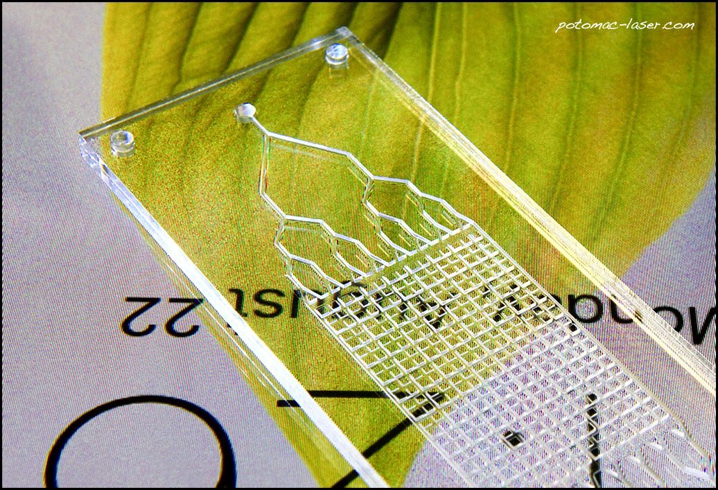
Rapid fabrication of microfluidic devices.
Use of pressure sensitive adhesive (PSA) layers for bonding and sealing is the simplest and most cost-effective available technique. Adhesive bonding additionally offers simple integration of non-similar standard or even nonconventional materials in microfluidic applications. In this approach, the layers of medical grade adhesive materials are first precisely patterned with a UV laser to allow inter-connection between the device layers. These adhesive sheets are then aligned and laminated between the device layers. A final specialty post-processing step for PSA bonded chips is also followed to improve the bonding quality and strength. The adhesive sealing and bonding process is further simplified by the use of specially formulated, commercially-available adhesive tapes.
Alternative bonding technologies, include solvent-assisted bonding, thermal bonding, and laser welding, depending on the materials and the constraints imposed by the final microfluidic application are possible.
Rapid Prototyping Microfluidic Devices
Micro-manufacturing processes such as laser micromachining, micro CNC machining and 3D Printing are all digital fabrication processes. A Computer Aided Design or CAD file instructs the tool on how to make the part. A significant benefit of CAD-based manufacturing is the ability to change designs and with no tooling or mold costs, produce a new part at low cost and in a short amount of time.