Biomedical applications have been the most challenging and exciting field for microfluidics, i.e. very small volumes of liquid flowing through channels ranging from tiny capillaries to 1 mm “pipelines”. Development of new drugs, genetic studies, point-of-care diagnostics, and fast analysis of air and water for presence of toxins and pathogens are just a few of the areas in which microfluidic product development is underway—and in which rapid prototyping is needed. A typical microfluidic system prototype consists of a fluid handling structure with miniature channels, wells, mixing structures, and connection ports that are coupled to external micropumps, microvalves, electronic modules, and similar actuation and analytical modules. The fluid handling structure is different in almost every application, and early stage prototyping and optimization of the system often requires construction of small quantities of several designs.
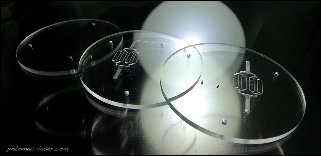
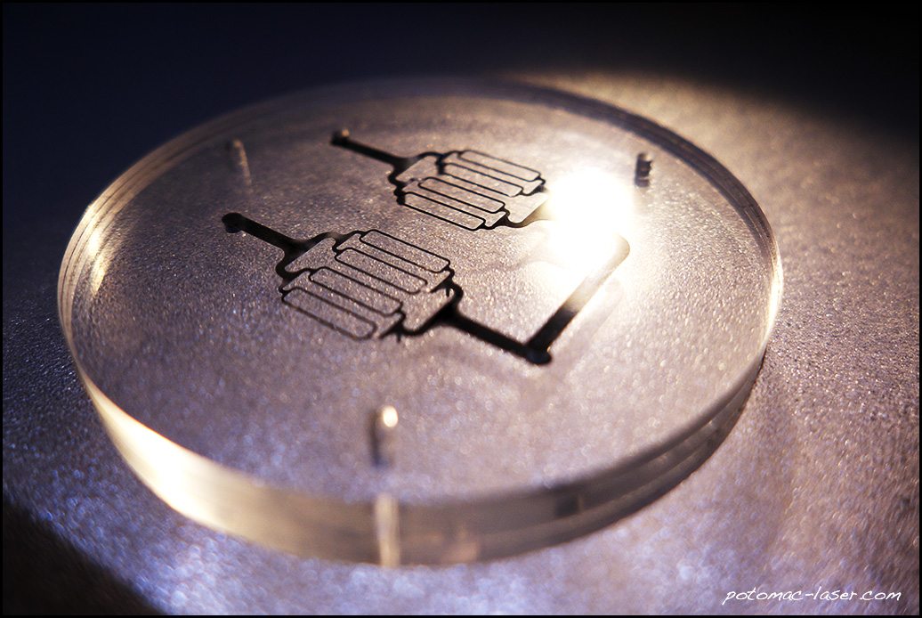
With rapid increasing in the design complexities of “lab-on-a-chip” systems, engineers are now considering multi-layer configuration for microfluidic devices as an interesting option that can complete more number of analyses on the same footprint of a cover-sealed single layer device. The basic concept in these designs is that one or multiple analysis steps can be performed within each layer of the device, and different layers are inter-connected via small through holes. Potomac has recently added this microfabrication capability to its digital toolbox in order to offer the fastest and most cost-effective microfluidic fabrication technologies to its customers.
The fabrication process utilizes a CAD drawing of the device submitted by the designer that is also used down in the road for quality control purposes. Potomac closely works with the customers to provide the drawings that can readily be used with applicable micro-fabrication systems. Depending on the specific design requirements, various available microfabrication tools such as lasers, micro-CNC, hot embossing, 3D printing, PDMS casting, etc. are used to process individual layers. Microfluidic components, for example microchannels as small as ~25µm in width and/or depth and via holes starting from <10µm in diameter, are patterned and finally the layers are cut into the desired contour. Quality control of the individual layers is also performed before integration that involves measurement of critical dimensions such as microchannel width, depth, and/or spacing and verification that channels and holes are free of contaminants and fine debris.
Individual layers of the device are first fabricated by using rapid microfabrication technologies such as lasers, micro-CNC, hot embossing, 3D printing, etc.
Alignment and bonding of the layers are critical steps in the fabrication of multi-layer devices. Use of pressure sensitive adhesive (PSA) layers for bonding and sealing is the simplest and most cost-effective available technique. Adhesive bonding additionally offers simple integration of non-similar standard or even nonconventional materials in microfluidic applications. In this approach, the layers of medical grade adhesive materials are first precisely patterned by UV laser to allow inter-connection between the device layers. These adhesive sheets are then aligned and laminated between the device layers. A final specialty post-processing step for PSA bonded chips is also followed to improve the bonding quality and strength. The adhesive sealing and bonding process is further simplified by the use of specially-formulated, commercially-available adhesive tapes that are utilized in Potomac’s quick turn process. Potomac also offers various alternative bonding technologies, including solvent-assisted bonding, thermal bonding, and laser welding, depending on the materials and the constraints imposed by the final microfluidic application.
Multiple layers of the device are precisely aligned and bonded by using various available bonding technologies.
This ongoing development work is in line with other Potomac microfabrication services aimed at providing designers with fast, low-cost approaches to fabricate microfluidic flow structures. The designers are now able to quickly explore new concepts in multi-layered configurations by digital fabrication of custom designs developed on their computers, submitted by internet, and fabricated in popular microfluidics materials. Potomac continues to offer full-service microfabrication services that help its customers to develop suitable prototyping and production processes for their new microfluidic designs.
Animal testing has long been an established protocol in drug discovery programs. But there are systemic issues with the far from reliable methodology. In fact, only 10% of the drugs that move from animal testing to human clinical trials succeeds. Such low yields increase the time and expense required to get pharmaceuticals to market, fueling…
In the field of microfluidics, where precision is key to innovation and application success, our expertise at Potomac Photonics sets a standard. We specialize in the art of laser drilling precise small holes in glass slides and coverslips, a critical capability for the fabrication of microfluidic devices. These devices play a pivotal role in various…
The world today seems consumed with fears about Artificial Intelligence, otherwise known as AI. Writers, journalists, ad copywriters, teachers, and artists are fearful their jobs will be lost to computers but in manufacturing we have been applying a subset of AI to manufacturing for decades with positive results. Like other forms of AI, Machine Learning…