Laser Cutting Silicon Wafers for NIST to Advance Solar Industry Standard
Laser cutting silicon wafers for NIST
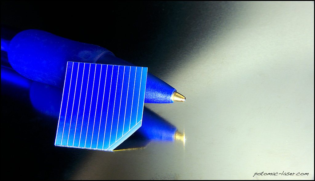
Potomac’s Photonics expertise in laser micromachining fragile materials helps NIST test new solar cells to ensure the solar energy industry’s manufacturing standards.
Solar energy is the fastest growing source of energy in the United States and the total install base is expanding exponentially. With explosive growth comes the need for better photovoltaic [PV] cells in order to successfully meet demand. Poor performing products are the kiss of death to any new industry, since new customers will not stay if promised results are not met.
In order to ensure solar cell performance, the National Institute of Standards and Technology [NIST] is performing tests for characterization and measurement of photovoltaic devices. As a non-regulatory part of the United State Department of Commerce, NIST is charged with promoting U.S. innovation and industrial competitiveness by advancing measurement science, standards, and technology. A number of programs guarantee parts and materials quality to ensure the success of American manufacturers, hopefully leading to a robust economy. In particular, NIST supports the Dept. of Energy’s National Renewable Energy Lab since NIST has more fundamental data and can take a proactive role in standards.
At NIST’s Heat Transfer and Alternative Energy Systems group in Gaithersburg, MD, research scientist Behrang Hamadani is designing tools to measure electrical performance of solar cells with a focus on metrology. “There is a lot of concern with the power conversion efficiency and performance of the PV panels, especially those built out of the country,” Behrang explains. “Consequently, we need to verify the specs and sometimes manufacturers need a highly calibrated reference against which to compare a new product. So we provide the industry with confidence in their own materials.”
Behrang has recently been working on a special solar cell on a single silicon wafer that was not packaged. Because it is easier to characterize a smaller area under simulation conditions, 2cm cells are the standard reference cell size. Needing to dice the wafer into smaller pieces, Behrang found Potomac Photonics who conveniently happened to be in Baltimore, a bit north of the NIST headquarters.
But proximity aside, Behrang came to the right place. The wafer was just 160 microns thick making it quite fragile and the proprietary material was susceptible to cracking, which would render the entire wafer useless due to stresses on the entire area. Behrang commented that dicing a wafer “sounds simple but being a new material, laser micromachining the wafer without cracking was a big issue for us.”
“Working with fragile materials such as thin silicon wafers or glass is a Potomac specialty,” adds Potomac President and CEO Mike Adelstein. “Potomac has development machining processes and parts handling that give our customers the results they need with no damage to the substrate.”
Potomac was excited to work on this exciting project with NIST. Hopefully, our laser cutting silicon wafers can help the world expand alternative energy sources to make the environment a healthier place for generations to come.
Animal testing has long been an established protocol in drug discovery programs. But there are systemic issues with the far from reliable methodology. In fact, only 10% of the drugs that move from animal testing to human clinical trials succeeds. Such low yields increase the time and expense required to get pharmaceuticals to market, fueling…
In the field of microfluidics, where precision is key to innovation and application success, our expertise at Potomac Photonics sets a standard. We specialize in the art of laser drilling precise small holes in glass slides and coverslips, a critical capability for the fabrication of microfluidic devices. These devices play a pivotal role in various…
The world today seems consumed with fears about Artificial Intelligence, otherwise known as AI. Writers, journalists, ad copywriters, teachers, and artists are fearful their jobs will be lost to computers but in manufacturing we have been applying a subset of AI to manufacturing for decades with positive results. Like other forms of AI, Machine Learning…